···
From 3D NAND to Logic Devices: A Process-Device Engineer's Perspective
Why people who span process-device are scarcer — and more valuable — in PIE / YE roles.
Stay tunedI'm Diamond. 11 years on the semiconductor production line — from 55nm down to 14nm logic, and from 32-layer to 196-layer 3D NAND, I took multiple product lines from zero to one and owned the full yield ramp-to-mass-production cycle. Not seen-it, done-it.
CVD thin-film (low-k / STI HARP / high-stress SiN) and CMOS devices — I've hit the wall on both. The hybrid process-device background lets me translate a process issue straight into device language to find root cause. 60+ patents and years of yield & failure triage notes are baked into the docs here.
Stuck on a process window that won't move, a resume that undersells you, or an interview "why" you can't nail? I can help turn that fuzzy instinct into an actionable plan and a story you can tell clearly.
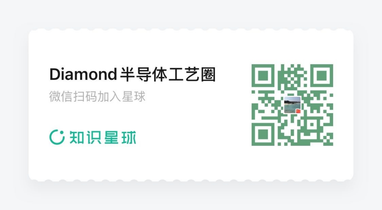
13 paid docs and consulting services, grouped by track. Buy & use instantly after payment.
Company landscape, core roles (CVD / device / PIE / YE / TD), interview hot topics, salary ranges and strategy. 11 yrs experience. PDF 9 pages.
8 modules ~50 questions (answers + analysis): process basics / CVD / CMOS / PIE / yield / reliability / EHS / behavioral. PDF 19 pages.
50 high-frequency CVD thin-film interview questions with analysis — vertical deep-dive for process roles.
NMOS strain engineering: PECVD stress tuning, UV cure, SMT integration and reliability trade-offs. PDF ~13 pages.
Etch selectivity, stress control and low-k-compatible integration, with optimized extended notes.
k-reduction physics, FSG / CDO / porous-ULK families, precursors, UV cure and PID mechanisms. PDF 22 pages.
k / stress / step-coverage / reliability trade-offs, Cu diffusion barrier applications and deposition window.
Ozone-TEOS, flowable oxide and void control, from shallow trench to inter-layer dielectric fill.
HCI / NBTI / PBTI / TDDB reliability + advanced module walkthrough. PDF 39 pages.
Nucleation, doping and thermal-management applications — semiconductor-grade diamond film report. PDF 42 pages.
6 questions covering process/device tech difficulties and career planning, with illustrated answers. ¥40 / 6 questions.
All 6 process reports in one bundle — best value for the full picture.
Continuously updated docs + real Q&A. Join once, benefit long-term.
Beyond the docs — a hands-on community for ongoing Q&A, frontier tracking, and real talk with peers.
Buying a doc is a one-time grab; joining the circle is compounding. Here I keep breaking down the process windows, stress trade-offs and defect mechanisms that docs can't fully cover and papers don't explain — straight from 11 years on the line. Your real fab questions get answered inside.
Latest job market intel and interview strategy
Diamond thin-film deposition process roundup
28nm/40nm logic CMOS device physics and failure analysis
ULK, low-k, STI HARP and other advanced CVD process notes
Scan with WeChat to join "Diamond Semiconductor Circle"
Turning front-line experience into deliverables. All services are based on open-domain knowledge and methodology — no confidential information from any former employer is involved.
Tailored to process / device / PIE / YE roles — restructure your résumé and quantify the impact so recruiters and interviewers see the highlights in 10 seconds.
View pricing →Role-play technical interviews based on real job descriptions — covering thin-film process, device physics, failure analysis and project deep-dives.
View pricing →Part-time advisory for equipment vendors, material suppliers and startups on thin-film process windows and device-structure reviews.
View pricing →Hands-on semiconductor thin-film process courses and public talks for new grads and career-switchers.
View pricing →Turning the pitfalls and the "aha" moments from the fab into reusable methodology.
Poor uniformity, particle contamination, step-coverage voids, film stress cracking, and abnormal electrical/composition. Each with its symptom, mechanism and debugging path.
Read more →Why low-k is needed, the properties it must satisfy, k-reduction physics, FSG / CDO / porous-ULK families, precursor chemistry, UV cure and PID mechanisms, and the core trade-off.
Read more →HCI / NBTI / PBTI / TDDB reliability degradation, plus STI, well engineering, salicide, SMT and low-k interconnect — systematically explained. Available as a PDF.
View the PDF →When HARP shows seam defects, the root cause is 80% upstream — not in the recipe. Plus the hidden substrate selectivity variable and the H2 treatment switch. Complete handbook with measured data, debug checklist, and 16 diagrams.
Read more →Why people who span process-device are scarcer — and more valuable — in PIE / YE roles.
Stay tunedCareer coaching, technical collaboration, content partnership — all welcome. Usually same-day reply on working days.

※ Powered by FormSubmit (third-party relay to my inbox). Used only to reply to your inquiry. I'll respond within one business day and share the download code via the contact you leave.
※ All collaboration is based on open-domain knowledge and personal experience, in compliance with confidentiality and non-compete requirements.